

Your electronic components cleared QC. The test reports look clean. The shipment left on time.
So why did three units fail in the field last month?
The answer most factories never find is sitting in a dispatch bay somewhere in the way a component was picked up, placed in a bin, or wrapped before it left the building. Electrostatic discharge leaves no visible mark. There’s no dent, no crack, no discolouration. The damage is inside the component, at the junction level, and it only shows up weeks or months later when the product is already in the customer’s hands.
For electronics manufacturers and component suppliers operating in cluster ESD packaging solutions in Ahmedabad are the difference between a clean field record and a warranty claim that costs ten times the value of the original component.
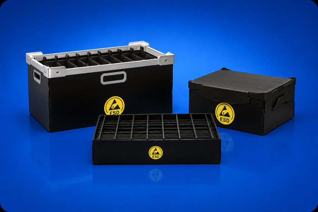
What ESD Damage Actually Looks Like And Why It’s So Hard to Catch
Electrostatic discharge damage comes in two forms, and only one of them is visible.
Hard failures are immediate the component stops working and gets caught at testing. These are frustrating but manageable. You find the problem, you reject the part, you move on
Latent failures are the real problem. The component sustains micro-level damage to its junction structure damage that doesn’t prevent it from passing functional testing, but that significantly shortens its operational life or makes it vulnerable to failure under normal operating stress. The component ships. It works. Then it doesn’t.
Latent ESD damage is estimated to account for a significant portion of electronics field failures globally, but it’s almost never identified as the root cause because by the time the failure occurs, the original packaging is long gone and the damage pathway is invisible. The only defence against latent failures is preventing the discharge in the first place which starts with the packaging your components travel in.
The Three Types of ESD Packaging And When Each One Applies
The terminology around ESD packaging is genuinely confusing, and misusing it leads to specification errors that cost money. Here is the practical breakdown:
Antistatic packaging
Resists the generation of static charge on its own surface. It does not shield the contents from external electrostatic fields. Surface resistance: above 10¹² ohms. Typical application: outer packaging layers, wrap material where the component is already inside an ESD protective container.
Static dissipative packaging
Allows any charge that builds up on the surface to flow slowly and safely to ground rather than discharging suddenly. Surface resistance: 10⁶ to 10¹¹ ohms. This is the specification most factories need for bins, trays, and storage containers within a defined EPA (Electrostatic Protected Area). The grey or charcoal-coloured bins you see on electronics production lines are almost always dissipative.
Conductive packaging
Allows charge to flow freely and rapidly. Surface resistance: below 10⁶ ohms. Used in specific high-risk applications typically where components need to be grounded rapidly during handling. Black carbon-loaded containers fall in this category.
Finding the Best ESD Packaging Solutions in Ahmedabad What to Actually Check
The ESD packaging market has a quality problem that isn’t visible to buyers who are evaluating on price alone. A bin that looks grey and carries an ESD label may or may not actually perform within the dissipative range especially after six months of use, cleaning, and UV exposure on the production floor.
Here is what a serious supplier evaluation for ESD packaging solutions in Ahmedabad should include:
- Surface resistance data
Ask for the measured surface resistance value not just the stated category. A legitimate manufacturer tests finished product and can provide batch-level documentation confirming the value falls within the specified range (10⁶ to 10¹¹ ohms for dissipative). - Material compliance certificate
This documents the additive loading used to achieve ESD performance. It matters for your own quality system records, especially if you’re supplying to automotive electronics OEMs or defence/aerospace customers who include packaging compliance in their supplier audits. - Post-cleaning performance
ESD performance can degrade when bins are cleaned with the wrong agents. Ask whether the supplier has data on resistance values after repeated cleaning with the agents you actually use isopropyl alcohol, water, or industrial detergents. A good supplier will have tested this. - Dimensional accuracy
ESD bins that stack poorly or have loose-fitting lids create handling risks that negate their protective function. Check that the bin you’re sampling is the same tooling and quality as what you’ll receive in bulk mould wear in lower-quality tooling produces bins that are dimensionally inconsistent across batches.
Building a Complete EPA ESD Packaging Is One Part of a System
This is where a lot of factories go wrong: they buy ESD bins and assume the problem is solved. ESD protection is a system, and packaging is one layer of it.
A functional EPA requires:
- Grounded flooring ESD-dissipative floor tiles or mats connected to a common ground point
- Operator grounding wrist straps or heel grounders worn by anyone handling sensitive components. A person in standard rubber-soled shoes on vinyl flooring can carry 35,000 volts
- Grounded workbench surfaces dissipative mats bonded to the common ground
- ESD-rated containers bins, trays, and racks within the zone that are either dissipative or conductive as specified
- EPA boundary controls clear physical or visual demarcation, with protocols for what enters the zone and how visitors are managed
Buying dissipative bins but running operators with no grounding is a half-measure. The charge they carry discharges through the component when they pick it up regardless of what the component is sitting in. A properly specified bin protects components in storage and transit. It doesn’t protect against an ungrounded operator during handling.
Common ESD Packaging Mistakes Gujarat Electronics Factories Make
Working with electronics manufacturers across Ahmedabad and Vadodara’s industrial clusters, these are the specification errors that come up most consistently:
- Assuming pink antistatic bags shield contents from external fields: they don’t. Pink antistatic bags protect against triboelectric charging from the bag surface itself. Metallic shielding bags are needed if you want to protect contents from external electrostatic fields during transit.
- Reusing shielding bags that have been torn or punctured: a metalized shielding bag with any breach in the film provides no shielding. Factories that reuse bags to reduce cost often don’t notice small tears, especially at corner folds. Replace shielding bags on every transit cycle for high-value components.
- Specifying ESD bins without specifying foam inserts: an ESD bin alone doesn’t protect against physical impact. If your components are fragile, the bin needs a dissipative or antistatic foam insert to hold the component in position. Using a standard EPE insert inside an ESD bin defeats the purpose if the foam is not ESD-rated.
Why Choose Shanti Polymers?
Shanti Polymers manufactures antistatic bins and ESD packaging solutions in-house at their Ahmedabad facility, with material compliance documentation available on request for quality audits. Their team works directly with purchase managers and quality leads to match bin specification material grade, surface resistance range, size, and foam fitment if required to the actual handling conditions in your plant.
ESD damage is almost always preventable, and it almost always gets prevented too late after a field failure report, after a customer audit, after a rejected batch. The specification decisions that determine your field failure rate are made on the packing line, not in the factory of the OEM your components eventually go into. Getting those decisions right starts with understanding what your packaging is actually doing and what it isn’t.
Contact Shanti Polymers for a free quote and material compliance information on ESD packaging solutions.